- RESEARCH BRIEFINGS
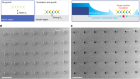
Semiconductor crystals grow from tiny nuclei, but the position of these nuclei is difficult to control precisely and can affect the crystal’s properties. An approach using ‘etching flux’ has now been developed that constrains the position at which a nucleus forms, enabling spatially programmable growth of large single crystals of semiconducting material.
This is a summary of: Park, J. et al. Spatially deterministic nucleation of 2D semiconductors by etching flux. Nature 658, 398–406 (2026).
doi: https://doi.org/10.1038/d41586-026-02934-2
‘Expert opinion’ and the figure are published under a CC BY 4.0 licence.
References
Mackus, A. J. M., Merkx, M. J. M. & Kessels, W. M. M. Chem. Mater. 31, 2–12 (2019).
Article PubMed Google Scholar
Ryu, S. W. et al. Curr. Appl. Phys. 16, 88–92 (2016).
Article Google Scholar
Kim, K. S. et al. Nature 614, 88–94 (2023).
Article PubMed Google Scholar
Download references
Related Articles
-
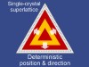 Read the paper: Spatially deterministic nucleation of 2D semiconductors by etching flux
-
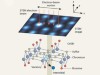 Targeted electron beam creates thousands of atomic crystal defects
-
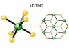 Mechanistic understanding and efficient engineering of crystal phases in 2D materials
Subjects
Latest on:
- Materials science
- Nanoscience and technology
-
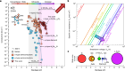
A 7-eV bandgap semiconductor based on silicon-doped α-(AlxGa1−x)2O3
Article
-
Spatially deterministic nucleation of 2D semiconductors by etching flux
Article
-
Semiconductors pushed into insulator territory
News & Views
-
Hydrogen bonding in water under extreme confinement
Article
-
Spatially deterministic nucleation of 2D semiconductors by etching flux
Article
-
A chiral superlattice route to spin-split topological antiferromagnetism
Article